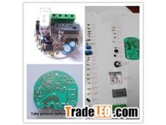
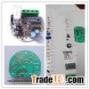


1. Real sample2. Schematic diagram and Overall configurations1.Take pictures before layout2.Remove the components from PCBA board,Website:http://www.oem-pcb.com, measure the parameter of components by digital electric bridge and multimeter.3.Grinding the solder mask on the pcb board4.Scan PCB wiring to the computer5.Adjust, copy the printing circuit board, then check and review.6.Do schematic diagram1.Fast PCB Fabrication for Samples and Mass Production2.Electronic Components Sourcing Servics3.PCBA Assembly Services:SMT,DIP,BGA...4.Function Test5.Stencil and Enclosure Assembly6.Standard Packin
PCB Layout Design

Shenzhen Sunsoar Tech Co.,Ltd
pcb assembly, Printed Circuit Boar
